What Is PCB Reverse Engineering and How Does It Work?

PCB reverse engineering is sometimes referred to as PCB copying, PCB cloning, and PCB duplication. It is a method of exploring technologies in reverse that is based on physically existing PCB boards.
In the process of PCB reverse engineering, which assumes that there are already physical objects and circuit boards of electronic products, the reverse analysis technology is used to analyze the circuit board in addition to the original product’s PCB file, bill of materials (BOM) file, schematic file, and any other production documents.
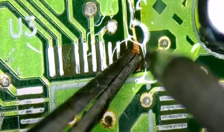
Such as PCB Gerber and PCB silk screen. This is done in the context of the presumption that there are already physical objects and circuit boards of electronic products. Then, to finish the complete copy of the original circuit board as a sample, utilize these engineering papers and production documentation for PCB re-production, component soldering, flying probe test, and circuit board debugging.
PCB Reverse Engineering and Its Possible Benefits PCB Design & Development
PCB reverse engineering is a technology that employs several reverse research approaches to get a PCB design, circuit schematic, and a BOM for an existing and working electronic format.
This technology falls under the category of reverse research. Because of technological advances, the creation of a new product that used to take two or three years may now be accomplished in as little as a few months. Previously, this process would take much longer.
In the most recent decade, the advancement of electronic technology has been changing with each passing day, and the majority of electronic devices have been changed at least once every year. Future upgrades for electrical products may happen more quickly.
How to Do Reverse Engineering on a Printed Circuit Board (PCB)
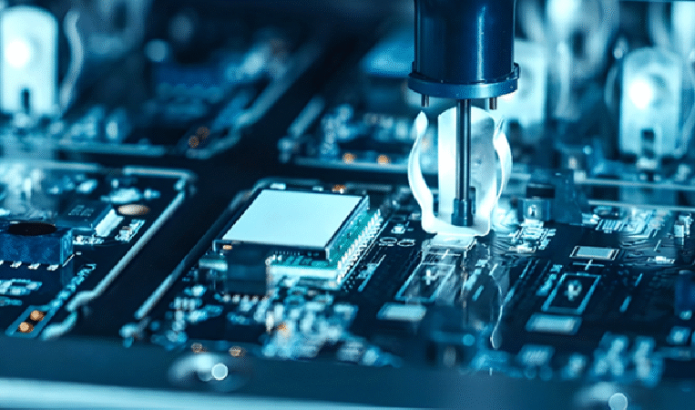
In the days when the software was available for PCB reverse engineering, the only way to respond was to sketch it out and measure it with a caliper. Both the speed and the accuracy were pretty bad. The pace was quite sluggish. In today’s world, doing reverse engineering on multi-layer plated through-hole boards using the software is a pretty straightforward process.
In most cases, you may start by scanning or photographing the PCB board, then you can enter the image into the program, and lastly, you can duplicate it using the protel99. After the patching is complete, it may be dumped into a format compatible with protel99.
The conversion of the PCB file to the schematic design will be the most challenging part of the process. It must have a wealth of experience for this task section to be finished as envisioned.
After completing the upper and lower layers, the finished layer located on the surface may be sanded with sandpaper. This exposes the inner layer gradually, and then a layer is placed, after which the coating is polished further until the process is accomplished.
Conclusion
Several professional PCB reverse engineering businesses in the market, such as Fast PCB Studio, can assist you in finishing the difficult PCB board cloning and reverse engineering process. It might be a valuable learning experience to try your hand at reverse engineering some more straightforward circuit boards on your own.