Bare PCB: Meaning, Manufacturing Process, and Why It Matters
A Bare PCB is the foundation of every electronic device, serving as the essential platform that connects components, enables signal flow, and ensures long-term reliability. Before any assembly, soldering, or component placement happens, the PCB exists in its purest form—fully fabricated but empty. This stage is critical because the quality of the Bare PCB directly determines the performance, durability, and safety of the final electronic product. Whether it’s consumer electronics, industrial equipment, medical devices, or automotive systems, understanding what a bare PCB is and how it is created helps you appreciate its importance in modern electronics.
What Is a Bare PCB?
A Bare PCB is a printed circuit board without any electronic components mounted on it. It contains only the copper traces, pads, vias, layers, and substrate materials needed for future assembly. It is “bare” because it arrives as a blank platform waiting for SMT or through-hole components to be installed. This board is manufactured using copper-clad laminates, etched circuitry, through-hole plating, and surface finishing processes, all of which prepare it for assembly. The accuracy of trace routing, via quality, layer alignment, and material selection directly impacts how well the finished circuit will function.
How a Bare PCB Is Manufactured
Design and Layer Preparation
The manufacturing of a Bare PCB begins with PCB layout design, where engineers define the copper routing, layer stack-up, pad geometry, and via structures. Once the design is finalized, the fabrication process moves into layer preparation. Each layer of the PCB is created by laminating copper sheets onto an insulating substrate such as FR-4, Rogers, or polyimide. Precise imaging techniques like laser direct imaging (LDI) are used to transfer the circuit pattern onto the copper surface.
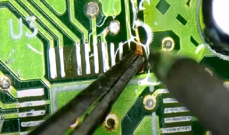
Etching, Drilling, and Plating
Once the circuit pattern is imaged, unwanted copper is removed through chemical etching to leave behind the desired traces. Drilling comes next and includes both mechanical drilling for through-holes and laser drilling for microvias in HDI boards. After drilling, plating is applied to create conductive pathways inside the holes, which is essential for multilayer interconnections. Proper plating thickness ensures reliability under thermal and electrical stress.
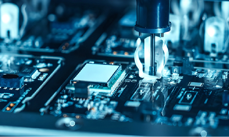
Lamination, Solder Mask, and Surface Finish
For multilayer Bare PCB manufacturing, the layers are laminated under high temperature and pressure to form a solid board. After lamination, solder mask is applied to insulate the copper traces and protect the board from oxidation and accidental solder bridging. The final step is adding a surface finish such as HASL, ENIG, OSP, or immersion silver to prepare the pads for future component soldering.
Why Bare PCB Quality Is So Important
A Bare PCB forms the structural backbone of an electronic device. If the board lacks precision, even the best assembly process cannot compensate for poor-quality copper routing, misaligned layers, or unreliable vias. High-quality bare PCBs minimize electrical losses, reduce EMI, withstand high temperatures, and ensure stable performance under tough conditions. In mission-critical applications such as aerospace, medical electronics, telecom equipment, and automotive systems, the bare PCB quality becomes even more crucial. The reliability of the final system depends on the accuracy and durability engineered into the bare board.
Applications of Bare PCB in Modern Electronics
The demand for Bare PCB products spans across multiple industries because every electronic device requires a stable foundation before assembly starts. Consumer appliances, industrial automation systems, LED lighting, EV chargers, IoT devices, and communication equipment all rely on high-quality bare PCBs. Advanced sectors like defense, robotics, and satellite communication use specialized materials and multilayer configurations to achieve superior performance. The flexibility of PCB manufacturing allows engineers to design boards that support high current, high frequency, miniaturization, and multi-functionality.
Choosing the Right Bare PCB for Your Project
Selecting the right Bare PCB depends on factors such as operating temperature, voltage requirements, signal integrity, impedance control, and mechanical durability. Material selection plays a major role—FR-4 is widely used for general applications, while ceramic, metal-core, Rogers, and polyimide materials are preferred for high-frequency or high-power environments. For complex designs, multilayer PCBs provide dense routing, reduced noise, and enhanced reliability. Getting the bare PCB right ensures smoother assembly, fewer defects, and longer product life.
Conclusion: Build Your Project on a Reliable Bare PCB
A Bare PCB is much more than a blank board; it is the precision-engineered foundation on which your entire electronic system depends. Whether you are developing prototypes or large-scale production runs, choosing a high-quality bare board will ensure stability, safety, and optimal performance. If you want consistent quality, professional engineering support, and reliable fabrication, partnering with an experienced Bare PCB manufacturer can make all the difference in your product’s success.