IC Substrate PCB: Structure, Importance, and Applications in Modern Electronics
An IC Substrate PCB is a high-density, high-precision printed circuit structure used as the base for packaging integrated circuits in advanced electronic devices. Unlike traditional PCBs, an IC Substrate PCB provides ultra-fine wiring, microvias, and stable electrical pathways between the semiconductor chip and the main circuit board. It serves as the intermediate layer that allows the chip to function efficiently while maintaining exceptional signal speed, reliability, and thermal stability. Because today’s electronics require faster data transmission and smaller device sizes, the role of the IC Substrate PCB has become foundational in semiconductor packaging technologies such as BGA, CSP, and flip-chip.
Why IC Substrate PCB Matters in Modern Technology
The significance of an IC Substrate PCB lies in its ability to bridge the gap between microscopic chip circuits and the comparatively larger and more robust PCB traces. As semiconductor geometry shrinks and device performance expectations rise, the demand for precise interconnection layers increases. IC Substrate PCBs offer controlled impedance, accurate signal distribution, and minimized parasitic effects, which are crucial for high-frequency, high-data-rate applications. Moreover, their thin dielectric layers and advanced materials ensure that heat is dissipated effectively, preventing thermal runaway in sensitive components. This combination of miniaturization, performance, and reliability makes them indispensable for processors, memory modules, network chips, and AI computing hardware.
How IC Substrate PCB Technology Works
Core Materials and Build-Up Layers
An IC Substrate PCB is created using advanced materials like BT resin, ABF (Ajinomoto Build-Up Film), or other high-performance epoxy systems. These materials allow the fabrication of extremely fine circuit patterns and ultra-thin dielectric layers. Build-up layers are added through sequential lamination, enabling multi-layer routing with microvias connecting each layer. This microvia technology allows extremely dense interconnections necessary for semiconductor packaging.
Fine-Line Circuit Formation
The performance of an IC Substrate PCB depends heavily on achieving ultra-fine line widths and spacing, often down to single-digit microns. Photolithography techniques and advanced etching processes ensure that the copper traces remain uniform and stable. This precision is essential for maintaining signal fidelity and supporting high-speed digital and RF systems.
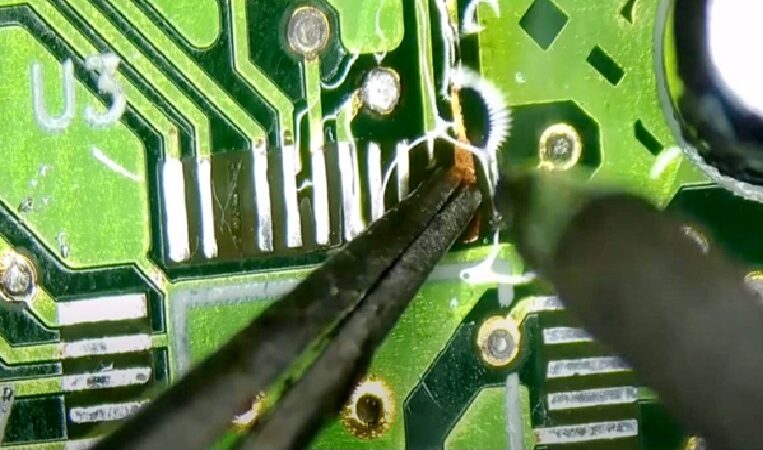
Microvia Drilling and Metallization
Microvias are drilled using laser technology due to their extremely small diameters. These microvias connect one build-up layer to another and are subsequently plated with copper to ensure strong electrical contact. The reliability of these vias directly affects the overall performance of the semiconductor package, making precision and plating uniformity critical.
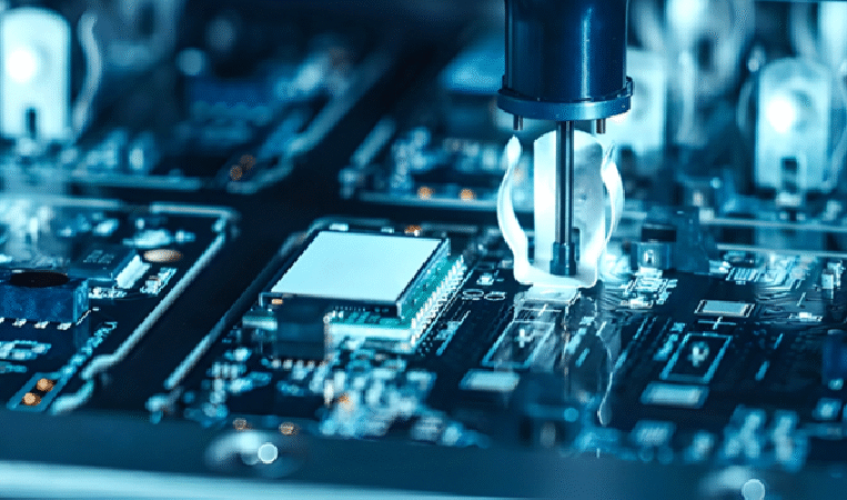
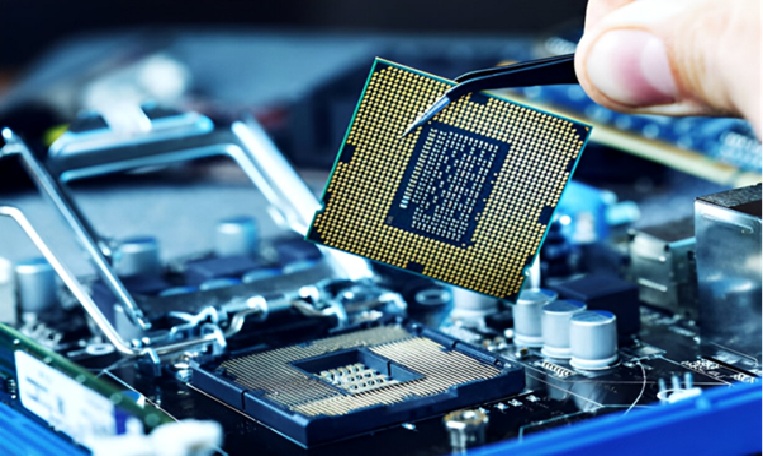
Surface Finish and Chip Attachment
The substrate surface receives finishes such as ENEPIG, ENIG, or immersion silver to promote excellent solderability. Depending on the packaging type, the chip may be attached with wire bonding, flip-chip bonding, or other advanced methods. The IC Substrate PCB must remain flat, cavity-free, and capable of withstanding high thermal cycles during chip bonding and reflow.
Advantages of IC Substrate PCB
Enhanced Electrical Performance
One of the greatest advantages of an IC Substrate PCB is its exceptional electrical characteristics. Controlled impedance pathways and short interconnect distances reduce signal delay, noise, and electromagnetic interference. This is vital for processors, memory units, and communication chips running at high frequencies.
Superior Heat Management
Because semiconductor devices generate significant heat, the IC Substrate PCB is engineered to conduct and dissipate thermal energy efficiently. High-performance resin systems and thermal vias ensure that heat travels away from the chip, improving reliability and extending component life.
Miniaturization and High Density
IC Substrate PCBs support the dense routing required for advanced semiconductor packages. With ultra-fine lines, microvias, and multi-layered structures, designers can pack more functionality into smaller footprints without sacrificing performance. This miniaturization is essential for smartphones, servers, wearable devices, and AI hardware.
Improved Mechanical Stability
In packaging, mechanical strength is as important as electrical precision. IC Substrate PCBs are engineered to withstand stress from thermal expansion, chip bonding, and repeated heating cycles. Their durability ensures stable connections, which is critical for long-term reliability in mission-critical electronics.
Applications of IC Substrate PCB
Smartphones and Consumer Electronics
Every high-performance processor in smartphones, tablets, and gaming devices depends on an IC Substrate PCB to enable high-speed computation and low-latency communication.
Servers, Data Centers, and AI Systems
AI processors, GPU accelerators, and high-speed networking chips rely heavily on IC substrates for their ability to manage high-frequency signals and maintain electrical stability under heavy workloads.
Automotive Electronics
Advanced driver-assistance systems (ADAS), radar modules, EV control units, and sensor fusion processors use IC Substrate PCBs to ensure precise signal control and long-term thermal reliability.
Medical and Aerospace Applications
Medical imaging systems, aerospace communication modules, and mission-critical navigation hardware use IC substrate technology for dependable performance and fault tolerance.
Design Considerations for IC Substrate PCB
Material Selection
Choosing between BT resin, ABF, or high-frequency materials depends on signal speed, thermal behavior, and mechanical requirements. Each material influences dielectric constant, loss tangent, and thermal expansion.
Microvia Reliability
With microvias being so small, manufacturers must ensure void-free plating and controlled drilling to avoid latent failures, especially in high-density interconnection designs.
Thermal Expansion Control
The CTE (Coefficient of Thermal Expansion) of the IC Substrate PCB must match that of the chip and main board to prevent mechanical stress and solder joint fatigue.
Precision in Fine-Line Fabrication
As line widths shrink, even minor variations can cause performance issues, making advanced photolithography and tight process control essential.
Conclusion: Build High-Performance Electronics With Precision IC Substrate PCB Technology
IC Substrate PCB technology is essential for developing modern electronic systems that demand speed, stability, and miniaturization. From smartphones and cloud computing to automotive and aerospace applications, IC substrates enable the next generation of powerful, reliable, and compact devices. If you are looking to achieve exceptional performance and long-term reliability in your semiconductor packaging projects, partnering with an experienced IC Substrate PCB Manufacturer will ensure the precision, quality, and expertise your designs require.